Micron Confidential and Proprietary
4GB, 8GB: e·MMC
Features
e·MMC Memory
MTFC4GACAANA-4M IT, MTFC4GACAALT-4M IT
MTFC8GACAANA-4M IT, MTFC8GACAALT-4M IT
Features
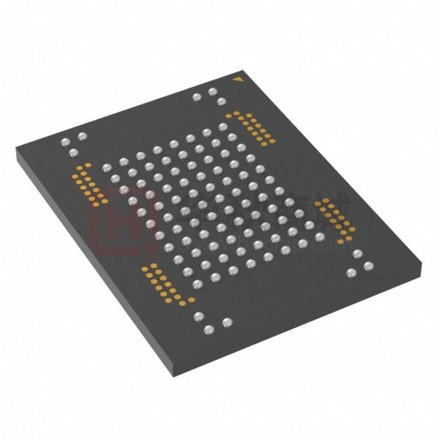
Figure 1: Micron e·MMC Device
• MultiMediaCard (MMC) controller and NAND Flash
• 100-ball TBGA
(RoHS compliant, "green" package)
• VCC: 2.7–3.6V
• VCCQ (dual voltage): 1.65–1.95V; 2.7–3.6V
• Temperature ranges
– Operating temperature: –40˚C to +85˚C
– Storage temperature: –40˚C to +85˚C
MMC
power
MMC controller
MMC
interface
MMC-Specific Features
• JEDEC/MMC standard version 4.51-compliant
(JEDEC Standard No. 84-B451) – SPI mode not
supported 1
– Advanced 11-signal interface
– x1, x4, and x8 I/Os, selectable by host
– SDR/DDR modes up to 52 MHz clock speed
– HS200 mode
– Real-time clock
– Command classes: class 0 (basic); class 2 (block
read); class 4 (block write); class 5 (erase);
class 6 (write protection); class 7 (lock card)
– Temporary write protection
– Boot operation (high-speed boot)
– Sleep mode
– Replay-protected memory block (RPMB)
– Secure erase and secure trim
– Hardware reset signal
– Multiple partitions with enhanced attribute
– Permanent and power-on write protection
– High-priority interrupt (HPI)
NAND Flash
power
MMC-Specific Features (Continued)
– Background operation
– Reliable write
– Discard and sanitize
– Extended partitioning
– Context ID
– Data TAG
– Packed commands
– Dynamic device capacity
– Backward compatible with previous MMC
– Thermal specification
– Cache
• ECC and block management implemented
Note:
09005aef856fbc21
emmc_ps8210_v451_80s_100b_it.pdf - Rev. E 06/18 EN
NAND Flash
1
1. The JEDEC specification is available at
www.jedec.org/sites/default/files/docs/
JESD84-B451.pdf.
Micron Technology, Inc. reserves the right to change products or specifications without notice.
© 2013 Micron Technology, Inc. All rights reserved.
Products and specifications discussed herein are subject to change by Micron without notice.
�Micron Confidential and Proprietary
4GB, 8GB: e·MMC
Features
e·MMC Performance and Current Consumption
Table 1: MLC Partition Performance
Typical Values
Condition1
4GB
8GB
Unit
Sequential write
11
24
MB/s
Sequential read
80
120
MB/s
Random write
1000
1000
IOPS
Random read
4000
4000
IOPS
Note:
1. Bus in x8 I/O and HS200 modes. Sequential access of 1MB chunk; random access of 4KB chunk over 1GB span.
Additional performance data, such as system performance on a specific application board, will be provided
in a separate document upon customer request.
Table 2: 52 MHz DDR2 Performance
Typical Values
Condition1
Sequential write
Sequential read
4GB
8GB
Unit
11
24
MB/s
75
80
MB/s
Random write
1000
1000
IOPS
Random read
3800
3800
IOPS
Note:
1. Bus in x8 I/O and 52 MHz DDR2 modes. Sequential access of 1MB chunk; random access of 4KB chunk over
1GB span. Additional performance data, such as system performance on a specific application board, will be
provided in a separate document upon customer request.
Table 3: Current Consumption
Typical Values (ICC/ICCQ)
Condition1
4GB
8GB
Unit
Write
50/20
60/20
mA
Read
60/60
60/60
mA
Sleep
0/180
0/180
uA
Auto-standby
25/150
50/180
uA
Note:
1. Bus in x8 I/O and HS200 modes. VCC = 3.6V and VCCQ = 1.95V. 25°C. Measurements done as average RMS current consumption. ICCQ in READ operation might be affected by tester load.
09005aef856fbc21
emmc_ps8210_v451_80s_100b_it.pdf - Rev. E 06/18 EN
2
Micron Technology, Inc. reserves the right to change products or specifications without notice.
© 2013 Micron Technology, Inc. All rights reserved.
�Micron Confidential and Proprietary
4GB, 8GB: e·MMC
Features
Part Numbering Information
Micron® e·MMC memory devices are available in different configurations and densities.
Figure 2: e·MMC Part Numbering
MT FC
xx
x
x
xx - xx
Micron Technology
Production Status
Product Family
Operating Temperature Range
FC = NAND Flash + controller
Package Codes
NAND Flash Density
Reserved
NAND Flash Component
Blank
Controller Revision
Table 4: Ordering Information
Base Part Number
Density
Package
Shipping
MTFC4GACAANA-4M IT
4GB
100-ball TBGA
14.0mm x 18.0mm x 1.2mm
Tray
Tape and reel
100-ball TBGA
14.0mm x 18.0mm x 1.2mm
Tape and reel
MTFC4GACAALT-4M IT
MTFC8GACAANA-4M IT
MTFC8GACAALT-4M IT
4GB
8GB
8GB
Tray
100-ball TBGA
14.0mm x 18.0mm x 1.2mm
Tray
Tape and reel
100-ball TBGA
14.0mm x 18.0mm x 1.2mm
Tape and reel
Tray
Device Marking
Due to the size of the package, the Micron-standard part number is not printed on the top of the device. Instead,
an abbreviated device mark consisting of a 5-digit alphanumeric code is used. The abbreviated device marks are
cross-referenced to the Micron part numbers at the FBGA Part Marking Decoder site: www.micron.com/decoder.
09005aef856fbc21
emmc_ps8210_v451_80s_100b_it.pdf - Rev. E 06/18 EN
3
Micron Technology, Inc. reserves the right to change products or specifications without notice.
© 2013 Micron Technology, Inc. All rights reserved.
�Micron Confidential and Proprietary
4GB, 8GB: e·MMC
Important Notes and Warnings
Important Notes and Warnings
Micron Technology, Inc. ("Micron") reserves the right to make changes to information published in this document,
including without limitation specifications and product descriptions. This document supersedes and replaces all
information supplied prior to the publication hereof. You may not rely on any information set forth in this document if you obtain the product described herein from any unauthorized distributor or other source not authorized
by Micron.
Automotive Applications. Products are not designed or intended for use in automotive applications unless specifically designated by Micron as automotive-grade by their respective data sheets. Distributor and customer/distributor shall assume the sole risk and liability for and shall indemnify and hold Micron harmless against all claims,
costs, damages, and expenses and reasonable attorneys' fees arising out of, directly or indirectly, any claim of
product liability, personal injury, death, or property damage resulting directly or indirectly from any use of nonautomotive-grade products in automotive applications. Customer/distributor shall ensure that the terms and conditions of sale between customer/distributor and any customer of distributor/customer (1) state that Micron
products are not designed or intended for use in automotive applications unless specifically designated by Micron
as automotive-grade by their respective data sheets and (2) require such customer of distributor/customer to indemnify and hold Micron harmless against all claims, costs, damages, and expenses and reasonable attorneys'
fees arising out of, directly or indirectly, any claim of product liability, personal injury, death, or property damage
resulting from any use of non-automotive-grade products in automotive applications.
Critical Applications. Products are not authorized for use in applications in which failure of the Micron component could result, directly or indirectly in death, personal injury, or severe property or environmental damage
("Critical Applications"). Customer must protect against death, personal injury, and severe property and environmental damage by incorporating safety design measures into customer's applications to ensure that failure of the
Micron component will not result in such harms. Should customer or distributor purchase, use, or sell any Micron
component for any critical application, customer and distributor shall indemnify and hold harmless Micron and
its subsidiaries, subcontractors, and affiliates and the directors, officers, and employees of each against all claims,
costs, damages, and expenses and reasonable attorneys' fees arising out of, directly or indirectly, any claim of
product liability, personal injury, or death arising in any way out of such critical application, whether or not Micron or its subsidiaries, subcontractors, or affiliates were negligent in the design, manufacture, or warning of the
Micron product.
Customer Responsibility. Customers are responsible for the design, manufacture, and operation of their systems,
applications, and products using Micron products. ALL SEMICONDUCTOR PRODUCTS HAVE INHERENT FAILURE RATES AND LIMITED USEFUL LIVES. IT IS THE CUSTOMER'S SOLE RESPONSIBILITY TO DETERMINE
WHETHER THE MICRON PRODUCT IS SUITABLE AND FIT FOR THE CUSTOMER'S SYSTEM, APPLICATION, OR
PRODUCT. Customers must ensure that adequate design, manufacturing, and operating safeguards are included
in customer's applications and products to eliminate the risk that personal injury, death, or severe property or environmental damages will result from failure of any semiconductor component.
Limited Warranty. In no event shall Micron be liable for any indirect, incidental, punitive, special or consequential
damages (including without limitation lost profits, lost savings, business interruption, costs related to the removal
or replacement of any products or rework charges) whether or not such damages are based on tort, warranty,
breach of contract or other legal theory, unless explicitly stated in a written agreement executed by Micron's duly
authorized representative.
09005aef856fbc21
emmc_ps8210_v451_80s_100b_it.pdf - Rev. E 06/18 EN
4
Micron Technology, Inc. reserves the right to change products or specifications without notice.
© 2013 Micron Technology, Inc. All rights reserved.
�Micron Confidential and Proprietary
4GB, 8GB: e·MMC
General Description
General Description
Micron e·MMC is a communication and mass data storage device that includes a MultiMediaCard (MMC) interface, a NAND Flash component, and a controller on an advanced 11-signal bus, which is compliant with the MMC system specification. Its low
cost, small size, Flash technology independence, and high data throughput make
e·MMC ideal for smartphones, digital cameras, PDAs, MP3s, and other portable applications.
The nonvolatile e·MMC draws no power to maintain stored data, delivers high performance across a wide range of operating temperatures, and resists shock and vibration disruption.
09005aef856fbc21
emmc_ps8210_v451_80s_100b_it.pdf - Rev. E 06/18 EN
5
Micron Technology, Inc. reserves the right to change products or specifications without notice.
© 2013 Micron Technology, Inc. All rights reserved.
�Micron Confidential and Proprietary
4GB, 8GB: e·MMC
Signal Descriptions
Signal Descriptions
Table 5: Signal Descriptions
Symbol
Type
Description
CLK
Input
Clock: Each cycle of the clock directs a transfer on the command line and on the data line(s). The
frequency can vary between the minimum and the maximum clock frequency.
RST_n
Input
Reset: The RST_n signal is used by the host for resetting the device, moving the device to the preidle state. By default, the RST_n signal is temporarily disabled in the device. The host must set ECSD
register byte 162, bits[1:0] to 0x1 to enable this functionality before the host can use it.
CMD
I/O
Command: This signal is a bidirectional command channel used for command and response transfers. The CMD signal has two bus modes: open-drain mode and push-pull mode (see Operating
Modes). Commands are sent from the MMC host to the device, and responses are sent from the
device to the host.
DAT[7:0]
I/O
Data I/O: These are bidirectional data signals. The DAT signals operate in push-pull mode. By default, after power-on or assertion of the RST_n signal, only DAT0 is used for data transfer. The
MMC controller can configure a wider data bus for data transfer either using DAT[3:0] (4-bit mode)
or DAT[7:0] (8-bit mode). e·MMC includes internal pull-up resistors for data lines DAT[7:1]. Immediately after entering the 4-bit mode, the device disconnects the internal pull-up resistors on the
DAT[3:1] lines. Upon entering the 8-bit mode, the device disconnects the internal pull-ups on the
DAT[7:1] lines.
VCC
Supply
VCC: NAND interface (I/F) I/O and NAND Flash power supply.
VCCQ
Supply
VCCQ: e·MMC controller core and e·MMC I/F I/O power supply.
VSS1
Supply
VSS: NAND I/F I/O and NAND Flash ground connection.
VSSQ1
Supply
VSSQ: e·MMC controller core and e·MMC I/F ground connection.
VDDIM
Internal voltage node: At least a 0.1μF capacitor is required to connect VDDIM to ground. A 1μF capacitor is recommended. Do not tie to supply voltage or ground.
NC
–
No connect: No internal connection is present.
RFU
–
Reserved for future use: No internal connection is present. Leave it floating externally.
Note:
09005aef856fbc21
emmc_ps8210_v451_80s_100b_it.pdf - Rev. E 06/18 EN
1. VSS and VSSQ are connected internally.
6
Micron Technology, Inc. reserves the right to change products or specifications without notice.
© 2013 Micron Technology, Inc. All rights reserved.
�Micron Confidential and Proprietary
4GB, 8GB: e·MMC
100-Ball Signal Assignments
100-Ball Signal Assignments
Figure 3: 100-Ball LFBGA (Top View, Ball Down)
1
2
A
NC
NC
B
NC
3
4
5
6
7
8
9
10
NC
NC
A
NC
B
D
RFU
RFU
RFU
RFU
RFU
RFU
RFU
RFU
D
E
RFU
RFU
VDDIM
RFU
RFU
RFU
RFU
RFU
E
F
VCC
VCC
VCC
VCC
VCC
VCC
VCC
VCC
F
G
VSS
VSS
VSS
VSS
VSS
VSS
VSS
VSS
G
H
VSSQ
VCCQ
RFU
RFU
RFU
RFU
VCCQ
VSSQ
H
J
RFU
RFU
RFU
RFU
RFU
RFU
RFU
RFU
J
K
DAT0
DAT2
RFU
RFU
RFU
RFU
DAT5
DAT7
K
L
VCCQ
VSSQ
VCCQ
RFU
RFU
VCCQ
VSSQ
VCCQ
L
M
RFU
RFU
VSSQ
RST_n
RFU
VSSQ
RFU
RFU
M
N
DAT1
DAT3
RFU
RFU
RFU
RFU
DAT4
DAT6
N
P
VSSQ
VCCQ
RFU
CMD
CLK
RFU
VCCQ
VSSQ
P
T
NC
U
NC
Notes:
09005aef856fbc21
emmc_ps8210_v451_80s_100b_it.pdf - Rev. E 06/18 EN
NC
NC
NC
T
NC
U
1. Connect a 1μF decoupling capacitor from VDDI to ground.
2. Some test pads on the device are not shown. They are not solder balls and are for Micron internal use only.
3. Some previous versions of the JEDEC product or mechanical specification had defined
reserved for future use (RFU) balls as no connect (NC) balls. NC balls assigned in the previous specifications could have been connected to ground on the system board. To enable new feature introduction, some of these balls are assigned as RFU in the v4.4 mechanical specification. Any new PCB footprint implementations should use the new ball
assignments and leave the RFU balls floating on the system board.
4. VCC, VCCQ, VSS, and VSSQ balls must all be connected.
7
Micron Technology, Inc. reserves the right to change products or specifications without notice.
© 2013 Micron Technology, Inc. All rights reserved.
�Micron Confidential and Proprietary
4GB, 8GB: e·MMC
Package Dimensions
Package Dimensions
Figure 4: 100-Ball TBGA – 14.0mm x 18.00mm x 1.2mm (Package Codes: NA, LT)
Seating
plane
0.12 A
A
100X Ø0.53
Solder ball
material: SAC305.
Dimensions apply
to solder balls postreflow on Ø0.5 SMD
ball pads.
1.01 ±0.1
10
9
8
7
6
5
4
3
2
Ball A1 ID
1
Ball A1 ID
A
B
D
E
F
G
H
16
CTR 1 TYP
J
18 ±0.1
K
L
M
N
P
T
U
1 TYP
1.1 ±0.1
9 CTR
0.31 MIN
Test pads.
Ni/Au plated.
No solder balls.
14 ±0.1
Note:
09005aef856fbc21
emmc_ps8210_v451_80s_100b_it.pdf - Rev. E 06/18 EN
1. Dimensions are in millimeters.
8
Micron Technology, Inc. reserves the right to change products or specifications without notice.
© 2013 Micron Technology, Inc. All rights reserved.
�Micron Confidential and Proprietary
4GB, 8GB: e·MMC
Architecture
Architecture
Figure 5: e.MMC Functional Block Diagram
e.MMC
MMC
controller
RST_n
VDDIM
VCCQM
Registers
CMD
CLK
VCCM
DAT[7:0]
OCR
CSD
RCA
CID
ECSD
DSR
VSS1
VSSQ1
NAND Flash
1. VSS and VSSQ are internally connected.
Note:
MMC Protocol Independent of NAND Flash Technology
The MMC specification defines the communication protocol between a host and a device. The protocol is independent of the NAND Flash features included in the device.
The device has an intelligent on-board controller that manages the MMC communication protocol.
The controller also handles block management functions such as logical block allocation and wear leveling. These management functions require complex algorithms and
depend entirely on NAND Flash technology (generation or memory cell type).
The device handles these management functions internally, making them invisible to
the host processor.
Defect and Error Management
Micron e.MMC incorporates advanced technology for defect and error management. If
a defective block is identified, the device completely replaces the defective block with
one of the spare blocks. This process is invisible to the host and does not affect data
space allocated for the user.
The device also includes a built-in error correction code (ECC) algorithm to ensure that
data integrity is maintained.
To make the best use of these advanced technologies and ensure proper data loading
and storage over the life of the device, the host must exercise the following precautions:
• Check the status after WRITE, READ, and ERASE operations.
• Avoid power-down during WRITE and ERASE operations.
09005aef856fbc21
emmc_ps8210_v451_80s_100b_it.pdf - Rev. E 06/18 EN
9
Micron Technology, Inc. reserves the right to change products or specifications without notice.
© 2013 Micron Technology, Inc. All rights reserved.
�Micron Confidential and Proprietary
4GB, 8GB: e·MMC
OCR Register
OCR Register
The 32-bit operation conditions register (OCR) stores the voltage profile of the card and
the access mode indication. In addition, this register includes a status information bit.
Table 6: OCR Parameters
OCR Bits
OCR Value
[31]
1b (ready)/0b (busy)1
[30:29]
10b
[28:24]
0 0000b
[23:15]
1 1111 1111b
2.7–3.6V voltage range
[14:8]
000 0000b
2.0–2.7V voltage range
[7]
1b
[6:0]
000 0000b
Note:
09005aef856fbc21
emmc_ps8210_v451_80s_100b_it.pdf - Rev. E 06/18 EN
Description
Device power-on status bit
Sector mode
Reserved
1.70–1.95V voltage range
Reserved
1. OCR = C0FF8080h after the device has completed power-up.
10
Micron Technology, Inc. reserves the right to change products or specifications without notice.
© 2013 Micron Technology, Inc. All rights reserved.
�Micron Confidential and Proprietary
4GB, 8GB: e·MMC
CID Register
CID Register
The card identification (CID) register is 128 bits wide. It contains the device identification information used during the card identification phase as required by e·MMC protocol. Each device is created with a unique identification number.
Table 7: CID Register Field Parameters
Name
Field
Width
CID Bits
CID Value
Manufacturer ID
MID
8
[127:120]
FEh
Reserved
–
6
[119:114]
–
Card/BGA
CBX
2
[113:112]
01h
OEM/application ID
OID
8
[111:104]
4Eh
Product name
PNM
48
[103:56]
P1xxxx
Product revision
PRV
8
[55:48]
–
Product serial number
PSN
32
[47:16]
–
Manufacturing date
MDT
8
[15:8]
–
CRC7 checksum
CRC
7
[7:1]
–
–
1
0
–
Not used; always 1
09005aef856fbc21
emmc_ps8210_v451_80s_100b_it.pdf - Rev. E 06/18 EN
11
Micron Technology, Inc. reserves the right to change products or specifications without notice.
© 2013 Micron Technology, Inc. All rights reserved.
�Micron Confidential and Proprietary
4GB, 8GB: e·MMC
CSD Register
CSD Register
The card-specific data (CSD) register provides information about accessing the device
contents. The CSD register defines the data format, error correction type, maximum data access time, and data transfer speed, as well as whether the DS register can be used.
The programmable part of the register (entries marked with W or E in the following table) can be changed by the PROGRAM_CSD (CMD27) command.
Table 8: CSD Register Field Parameters
Size
(Bits)
Cell
Type1
CSD
Bits
CSD
Value
CSD_STRUCTURE
2
R
[127:126]
03h
SPEC_VERS
4
R
[125:122]
04h
2
–
[121:120]
–
Name
Field
CSD structure
System specification version
Reserved2
–
Data read access time 1
TAAC
8
R
[119:112]
4Fh
Data read access time 2 in CLK cycles
(NSAC × 100)
NSAC
8
R
[111:104]
01h
Maximum bus clock frequency
TRAN_SPEED
8
R
[103:96]
32h
CCC
12
R
[95:84]
0F5h
Maximum read data block length
READ_BL_LEN
4
R
[83:80]
09h
Partial blocks for reads supported
READ_BL_PARTIAL
1
R
[79]
0h
Write block misalignment
WRITE_BLK_MISALIGN
1
R
[78]
0h
Read block misalignment
READ_BLK_MISALIGN
1
R
[77]
0h
DSR_IMP
1
R
[76]
1h
2
–
[75:74]
–
Card command
DSR
classes3
implemented4
Reserved
–
Device size
C_SIZE
12
R
[73:62]
FFFh
Maximum read current at VDD,min
VDD_R_CURR_MIN
3
R
[61:59]
07h
Maximum read current at VDD,max
VDD_R_CURR_MAX
3
R
[58:56]
07h
Maximum write current at VDD,min
VDD_W_CURR_MIN
3
R
[55:53]
07h
Maximum write current at VDD,max
VDD_W_CURR_MAX
3
R
[52:50]
07h
Device size multiplier
C_SIZE_MULT
3
R
[49:47]
07h
Erase group size
ERASE_GRP_SIZE
5
R
[46:42]
1Fh
Erase group size multiplier
ERASE_GRP_MULT
5
R
[41:37]
1Fh
Write protect group size
WP_GRP_SIZE
5
R
[36:32]
07h
4GB
8GB
0Fh
16GB
1Fh
Write protect group enable
WP_GRP_ENABLE
1
R
[31]
1h
Manufacturer default ECC
DEFAULT_ECC
2
R
[30:29]
00h
Write-speed factor
R2W_FACTOR
3
R
[28:26]
02h
Maximum write data block length
WRITE_BL_LEN
4
R
[25:22]
09h
Partial blocks for writes supported
WRITE_BL_PARTIAL
1
R
[21]
0h
4
–
[20:17]
–
1
R
[16]
0h
Reserved
Content protection application
09005aef856fbc21
emmc_ps8210_v451_80s_100b_it.pdf - Rev. E 06/18 EN
–
CONTENT_PROT_APP
12
Micron Technology, Inc. reserves the right to change products or specifications without notice.
© 2013 Micron Technology, Inc. All rights reserved.
�Micron Confidential and Proprietary
4GB, 8GB: e·MMC
CSD Register
Table 8: CSD Register Field Parameters (Continued)
Size
(Bits)
Cell
Type1
CSD
Bits
CSD
Value
FILE_FORMAT_GRP
1
R/W
[15]
0h
Copy flag (OTP)
COPY
1
R/W
[14]
0h
Permanent write protection
PERM_WRITE_PROTECT
1
R/W
[13]
0h
Temporary write protection
TMP_WRITE_PROTECT
1
R/W/E
[12]
0h
File format
FILE_FORMAT
2
R/W
[11:10]
00h
ECC
ECC
2
R/W/E
[9:8]
00h
CRC
CRC
7
R/W/E
[7:1]
47h
Name
Field
File-format group
Reserved
4GB
–
Notes:
5Fh
16GB
6Fh
1
–
[0]
–
1. R = Read-only;
R/W = One-time programmable and readable;
R/W/E = Multiple writable with value kept after a power cycle, assertion of the RST_n
signal, and any CMD0 reset, and readable
2. Reserved bits should be read as 0.
3. CM0 restriction: CMD0 (SW RESET) is not supported during programming command. If
SW RESET is issued during programming commands, a power cycle is required.
4. The IPEAK, max driving capability can be modified according to the actual capacitive load
on the e·MMC interface signals in the user application board, using CMD4. In HS200
mode, the driver strength value is set in EXT_CSD[185], using CMD6.
CMD4 Argument
0x01000000
0x02000000
0x04000000
0x08000000
0x10000000
0x20000000
0x40000000
0x80000000
09005aef856fbc21
emmc_ps8210_v451_80s_100b_it.pdf - Rev. E 06/18 EN
8GB
Driving Capability (mA)
4
8
12 (default)
16
20
24
28
32
13
Micron Technology, Inc. reserves the right to change products or specifications without notice.
© 2013 Micron Technology, Inc. All rights reserved.
�Micron Confidential and Proprietary
4GB, 8GB: e·MMC
ECSD Register
ECSD Register
The 512-byte extended card-specific data (ECSD) register defines device properties and
selected modes. The most significant 320 bytes are the properties segment. This segment defines device capabilities and cannot be modified by the host. The lower 192
bytes are the modes segment. The modes segment defines the configuration in which
the device is working. The host can change the properties of modes segments using the
SWITCH command.
Table 9: ECSD Register Field Parameters
Name
Field
Size
(Bytes)
Cell
Type1
ECSD
Bytes
ECSD
Value
–
6
–
[511:506]
–
Properties Segment
Reserved2
Extended security protocol
EXT_SECURITY_ERR
1
R
[505]
00h
Supported command sets
S_CMD_SET
1
R
[504]
01h
HPI features
HPI_FEATURES
1
R
[503]
03h
Background operations support
BKOPS_SUPPORT
1
R
[502]
01h
Max-packed read commands
MAX_PACKED_READS
1
R
[501]
3Ch
Max-packed write commands
MAX_PACKED_WRITES
1
R
[500]
3Ch
Data tag support
DATA_TAG_SUPPORT
1
R
[499]
01h
Tag unit size
TAG_UNIT_SIZE
1
R
[498]
03h
Tag resources size
TAG_RES_SIZE
1
R
[497]
00h
Context management capabilities
CONTEXT_CAPABILITIES
1
R
[496]
05h
Large unit size
LARGE_UNIT_SIZE_M1
1
R
[495]
03h
4GB
8GB
Extended partitions attribute support
EXT_SUPPORT
Reserved
07h
1
[494]
03h
241
–
[493:253]
–
Cache size
CACHE_SIZE
4
R
[252:249]
00000020h
Generic CMD6 timeout
GENERIC_CMD6_TIME
1
R
[248]
19h
Power-off notification (long) timeout
POWER_OFF_LONG_TIME
1
R
[247]
FFh
Background operations status
BKOPS_STATUS
1
R
[246]
00h
Number of correctly programmed sectors
CORRECTLY_PROG_SECTORS_NUM
4
R
[245:242]
00000000h
First initialization time after partitioning (first CMD1 to device ready)
INI_TIMEOUT_AP
1
R
[241]
32h
–
1
–
[240]
–
Reserved
–
R
Power class for 52 MHz, DDR at 3.6V
PWR_CL_DDR_52_360
1
R
[239]
04h
Power class for 52 MHz, DDR at 1.95V
PWR_CL_DDR_52_195
1
R
[238]
09h
Power class for 200 MHz at 1.95V
PWR_CL_200_195
1
R
[237]
09h
Power class for 200 MHz, at 1.3V
PWR_CL_200_130
1
R
[236]
00h
Minimum write performance for 8-bit
at 52 MHz in DDR mode
MIN_PERF_DDR_W_8_52
1
R
[235]
00h
09005aef856fbc21
emmc_ps8210_v451_80s_100b_it.pdf - Rev. E 06/18 EN
14
Micron Technology, Inc. reserves the right to change products or specifications without notice.
© 2013 Micron Technology, Inc. All rights reserved.
�Micron Confidential and Proprietary
4GB, 8GB: e·MMC
ECSD Register
Table 9: ECSD Register Field Parameters (Continued)
Size
(Bytes)
Cell
Type1
ECSD
Bytes
ECSD
Value
Minimum read performance for 8-bit at MIN_PERF_DDR_R_8_52
52 MHz in DDR mode
1
R
[234]
00h
Reserved
1
–
[233]
–
Name
Field
–
TRIM multiplier
TRIM_MULT
1
R
[232]
03h
Secure feature support
SEC_FEATURE_SUPPORT
1
R
[231]
55h
Secure erase multiplier
SEC_ERASE_MULT
1
R
[230]
06h
Secure trim multiplier
SEC_TRIM_MULT
1
R
[229]
09h
Boot information
BOOT_INFO
1
R
[228]
07h
Reserved
Boot partition size
–
BOOT_SIZE_MULT
4GB
1
–
[227]
–
1
R
[226]
80h
8GB
Access size
ACC_SIZE
4GB
High-capacity erase unit size
HC_ERASE_GRP_SIZE
80h
1
R
[225]
1
R
[224]
8GB
4GB
06h
07h
8GB
08h
10h
High-capacity erase timeout
ERASE_TIMEOUT_MULT
1
R
[223]
01h
Reliable write-sector count
REL_WR_SEC_C
1
R
[222]
01h
High-capacity write protect group size
HC_WP_GRP_SIZE
1
R
[221]
01h
Sleep current (VCC)
S_C_VCC
1
R
[220]
06h
Sleep current (VCCQ)
S_C_VCCQ
1
R
[219]
09h
1
–
[218]
–
1
R
[217]
10h
1
–
[216]
–
4
R
[215:212]
00734000h
1
–
[211]
–
1
R
[210]
08h
Minimum read performance for 8-bit at MIN_PERF_R_8_52
52 MHz
1
R
[209]
08h
Minimum write performance for 8-bit
at 26 MHz and 4-bit at 52 MHz
1
R
[208]
08h
Minimum read performance for 8-bit at MIN_PERF_R_8_26_4_52
26 MHz and 4-bit at 52 MHz
1
R
[207]
08h
Minimum write performance for 4-bit
at 26 MHz
1
R
[206]
08h
Minimum read performance for 4-bit at MIN_PERF_R_4_26
26 MHz
1
R
[205]
08h
Reserved
1
–
[204]
–
Reserved
Sleep/awake timeout
–
S_A_TIMEOUT
Reserved
Sector count
–
SEC_COUNT
4GB
8GB
Reserved
Minimum write performance for 8-bit
at 52 MHz
09005aef856fbc21
emmc_ps8210_v451_80s_100b_it.pdf - Rev. E 06/18 EN
–
MIN_PERF_W_8_52
MIN_PERF_W_8_26_4_52
MIN_PERF_W_4_26
–
15
00E68000h
Micron Technology, Inc. reserves the right to change products or specifications without notice.
© 2013 Micron Technology, Inc. All rights reserved.
�Micron Confidential and Proprietary
4GB, 8GB: e·MMC
ECSD Register
Table 9: ECSD Register Field Parameters (Continued)
Name
Field
Size
(Bytes)
Cell
Type1
ECSD
Bytes
ECSD
Value
Power class for 26 MHz at 3.6V
PWR_CL_26_360
1
R
[203]
02h
Power class for 52 MHz at 3.6V
PWR_CL_52_360
1
R
[202]
02h
Power class for 26 MHz at 1.95V
PWR_CL_26_195
1
R
[201]
05h
Power class for 52 MHz at 1.95V
PWR_CL_52_195
1
R
[200]
05h
Partition switching timing
PARTITION_SWITCH_TIME
1
R
[199]
03h
Out-of-interrupt busy timing
OUT_OF_INTERRUPT_TIME
1
R
[198]
0Ah
I/O driver strength
DRIVER_STRENGTH
1
R
[197]
0Fh
Card type
CARD_TYPE
1
R
[196]
17h
1
–
[195]
–
1
R
[194]
02h
1
–
[193]
–
EXT_CSD_REV
1
R
[192]
06h
CMD_SET
1
R/W/E_P
[191]
00h
1
–
[190]
–
1
R
[189]
00h
1
–
[188]
–
1
R/W/E_P
[187]
00h
1
–
[186]
–
1
R/W/E_P
[185]
00h
1
–
[184]
–
1
W/E_P
[183]
00h
1
–
[182]
–
1
R
[181]
00h
1
–
[180]
–
Reserved
–
CSD structure version
CSD_STRUCTURE
Reserved
–
Extended CSD revision
Modes Segment
Command set
Reserved
–
Command set revision
CMD_SET_REV
Reserved
–
Power class
POWER_CLASS
Reserved
High-speed interface
–
timing4
HS_TIMING
Reserved
Bus width mode
–
BUS_WIDTH
Reserved
Erased memory content
–
ERASED_MEM_CONT
Reserved
–
Partition configuration
PARTITION_CONFIG
1
R/W/E,
R/W/E_P
[179]
00h
Boot configuration protection
BOOT_CONFIG_PROT
1
R/W,
R/W/C_P
[178]
00h
Boot bus width
BOOT_BUS_WIDTH
1
R/W/E
[177]
00h
1
–
[176]
–
Reserved
–
High-density erase group definition
ERASE_GROUP_DEF
1
R/W/E_P
[175]
00h
Boot write protection status registers
BOOT_WP_STATUS
1
R
[174]
00h
Boot area write protection register
BOOT_WP
1
R/W,
R/W/C_P
[173]
00h
1
–
[172]
–
Reserved
09005aef856fbc21
emmc_ps8210_v451_80s_100b_it.pdf - Rev. E 06/18 EN
–
16
Micron Technology, Inc. reserves the right to change products or specifications without notice.
© 2013 Micron Technology, Inc. All rights reserved.
�Micron Confidential and Proprietary
4GB, 8GB: e·MMC
ECSD Register
Table 9: ECSD Register Field Parameters (Continued)
Name
User write protection register
Field
USER_WP
Reserved
–
Size
(Bytes)
Cell
Type1
ECSD
Bytes
ECSD
Value
1
R/W,
R/W/C_P,
R/W/E_P
[171]
00h
1
–
[170]
–
R/W
[169]
00h
Firmware configuration
FW_CONFIG
1
RPMB size
RPMB_SIZE_MULT
1
R
[168]
01h
Write reliability setting register3
WR_REL_SET
1
R/W
[167]
00h
Write reliability parameter register
WR_REL_PARAM
1
R
[166]
05h
SANITIZE START operation
SANITIZE_START
1
W/E_P
[165]
00h
Manually start background operations
BKOPS_START
1
W/E_P
[164]
00h
Enable background operations handshake
BKOPS_EN
1
R/W
[163]
00h
Hardware reset function
RST_n_FUNCTION
1
R/W
[162]
00h
HPI management
HPI_MGMT
1
R/W/E_P
[161]
00h
Partitioning support
PARTITIONING_SUPPORT
1
R
[160]
07h
Maximum enhanced area size
MAX_ENH_SIZE_MULT
3
R
[159:157]
0001CDh
Partitions attribute
PARTITIONS_ATTRIBUTE
1
R/W
[156]
00h
Partitioning setting
PARTITION_SETTING_COMPLETED
1
R/W
[155]
00h
General-purpose partition size
GP_SIZE_MULT_GP3
12
R/W
[154:152]
000000h
GP_SIZE_MULT_GP2
[151:149]
000000h
GP_SIZE_MULT_GP1
[148:146]
000000h
GP_SIZE_MULT_GP0
[145:143]
000000h
Enhanced user data area size
ENH_SIZE_MULT
3
R/W
[142:140]
000000h
Enhanced user data start address
ENH_START_ADDR
4
R/W
[139:136]
00000000h
1
–
[135]
–
1
R/W
[134]
00h
Reserved
Bad block management mode
Reserved
–
SEC_BAD_BLK_MGMNT
1
–
[133]
–
Package case temperature is controlled TCASE_SUPPORT
–
1
W/E_P
[132]
00h
Periodic wake-up
1
R/W/E
[131]
00h
1
R
[130]
01h
PERIODIC_WAKEUP
Program CID/CSD in DDR mode support PROGRAM_CID_CSD_DDR_SUPPORT
Reserved
2
TBD
[129:128]
TBD
Vendor specific fields
VENDOR_SPECIFIC_FIELD
64
[127:64]
TBD
Native sector size
NATIVE_SECTOR_SIZE
1
R
[63]
00h
Sector size emulation
USE_NATIVE_SECTOR
1
R/W
[62]
00h
Sector size
DATA_SECTOR_SIZE
1
R
[61]
00h
1st initialization after disabling sector
size emulation
INI_TIMEOUT_EMU
1
R
[60]
0Ah
09005aef856fbc21
emmc_ps8210_v451_80s_100b_it.pdf - Rev. E 06/18 EN
–
17
Micron Technology, Inc. reserves the right to change products or specifications without notice.
© 2013 Micron Technology, Inc. All rights reserved.
�Micron Confidential and Proprietary
4GB, 8GB: e·MMC
ECSD Register
Table 9: ECSD Register Field Parameters (Continued)
Name
Field
Size
(Bytes)
Cell
Type1
ECSD
Bytes
ECSD
Value
Class 6 commands control
CLASS_6_CTRL
1
R/W/E_P
[59]
00h
Number of addressed group to be released
DYNCAP_NEEDED
1
R
[58]
00h
Exception events control
EXCEPTION_EVENTS_CTRL
2
R/W/E_P
[57:56]
00h
Exception events status
EXCEPTION_EVENTS_STATUS
2
R
[55:54]
00h
Extended partitions attribute
EXT_PARTITIONS_ATTRIBUTE
2
R/W
[53:52]
00h
Context configuration
CONTEXT_CONF
15
R/W/E_P
[51:37]
00h
Packed command status
PACKED_COMMAND_STATUS
1
R
[36]
00h
Packed command failure index
PACKED_FAILURE_INDEX
1
R
[35]
00h
Power-off notification
POWER_OFF_NOTIFICATION
1
R/W/E_P
[34]
00h
Control to turn the Cache ON/OFF
CACHE_CTRL
1
R/W/E_P
[33]
00h
Flushing of the cache
FLUSH_CACHE
1
W/E_P
[32]
00h
32
TBD
[31:0]
–
Reserved
–
Notes:
09005aef856fbc21
emmc_ps8210_v451_80s_100b_it.pdf - Rev. E 06/18 EN
1. R = Read-only;
R/W = One-time programmable and readable;
R/W/E = Multiple writable with the value kept after a power cycle, assertion of the
RST_n signal, and any CMD0 reset, and readable;
R/W/C_P = Writable after the value is cleared by a power cycle and assertion of the
RST_n signal (the value not cleared by CMD0 reset) and readable;
R/W/E_P = Multiple writable with the value reset after a power cycle, assertion of the
RST_n signal, and any CMD0 reset, and readable;
W/E_P = Multiple writable with the value reset after power cycle, assertion of the RST_n
signal, and any CMD0 reset, and not readable
2. Reserved bits should be read as 0.
3. Micron has tested power failure under best-application knowledge conditions with positive results. Customers may request a dedicated test for their specific application condition. Micron set this register during factory test and used the one-time programming
option.
4. tIH parameter in HS200 is 1.4ns. Refer to the JEDEC specification for the output timing
diagram.
18
Micron Technology, Inc. reserves the right to change products or specifications without notice.
© 2013 Micron Technology, Inc. All rights reserved.
�Micron Confidential and Proprietary
4GB, 8GB: e·MMC
DC Electrical Specifications – Device Power
DC Electrical Specifications – Device Power
The device current consumption for various device configurations is defined in the
power class fields of the ECSD register.
VCC is used for the NAND Flash device and its interface voltage; V CCQ is used for the
controller and the e·MMC interface voltage.
Figure 6: Device Power Diagram
VCCM
VCCQM
C3
C4
C1
C2
RST_n
Core regulator
NAND
control signals
CLK
CMD
DAT[7:0]
C6
NAND Flash
NAND
I/O block
C5
MMC
I/O block
VDDIM
Core
logic block
NAND
data bus
VCCQM
MMC controller
VCCQM
Table 10: Absolute Maximum Ratings
Parameters
Symbol
Min
Max
Unit
Voltage input
VIN
–0.6
4.6
V
VCC supply
VCC
–0.6
4.6
V
VCCQ supply
VCCQ
–0.6
4.6
V
Table 11: Power Domains
Parameter
Symbol
Comments
Host interface
VCCQM
High voltage range = 3.3V (nominal)
Low voltage range = 1.8V (nominal)
Memory
VCCM
High voltage range = 3.3V (nominal)
Internal
VDDIM
The internal regulator connection to an external decoupling capacitor
09005aef856fbc21
emmc_ps8210_v451_80s_100b_it.pdf - Rev. E 06/18 EN
19
Micron Technology, Inc. reserves the right to change products or specifications without notice.
© 2013 Micron Technology, Inc. All rights reserved.
�Micron Confidential and Proprietary
4GB, 8GB: e·MMC
DC Electrical Specifications – Device Power
Table 12: Capacitor and Resistance Specifications
Parameter
Symbol
Min
Max
Typ
Units
Notes
Pull-up resistance: CMD
R_CMD
4.7
50
10
kΩ
1
R_DAT
10
50
50
kΩ
1
R_RST_n
4.7
50
50
kΩ
2
45
55
50
Ω
3
SR_CLK
0
47
22
Ω
C1
2.2
4.7
2.2
µF
4
C2
0.1
0.22
0.1
C3
2.2
4.7
2.2
µF
5
C4
0.1
0.22
0.1
C3
2.2
4.7
4.7
µF
5
C4
0.1
0.22
0.22
C5
1
4.7
1
µF
6
C6
0.1
0.1
0.1
Pull-up resistance: DAT[7:0]
Pull-up resistance: RST_n
CLK/CMD/DAT[7:0] impedance
Serial resistance on CLK
VCCQ capacitor
VCC capacitor (≤8GB)
VCC capacitor (>8GB)
VDDIM capacitor (Creg)
Notes:
09005aef856fbc21
emmc_ps8210_v451_80s_100b_it.pdf - Rev. E 06/18 EN
1. Used to prevent bus floating.
2. If host does not use H/W RESET (RST_n), pull-up resistance is not needed on RST_n line
(Extended_CSD[162] = 00h).
3. Impedance match.
4. The coupling capacitor should be connected with VCCQ and VSSQ as closely as possible.
5. The coupling capacitor should be connected with VCC and VSS as closely as possible.
6. The coupling capacitor should be connected with VDDIM and VSS as closely as possible.
20
Micron Technology, Inc. reserves the right to change products or specifications without notice.
© 2013 Micron Technology, Inc. All rights reserved.
�Micron Confidential and Proprietary
4GB, 8GB: e·MMC
Revision History
Revision History
Rev. E – 06/18
• Added Important Notes and Warnings section for further clarification aligning to industry standards
• Added new MPNs
Rev. D – 08/15
• To Production status
Rev. C – 05/14
• Updated the operating temperature range and tIH spec
Rev. B – 04/14
• Added the "Absolute Maximum Ratings" table to the DC Electrical Specifications section
Rev. A – 10/13
• Initial release
8000 S. Federal Way, P.O. Box 6, Boise, ID 83707-0006, Tel: 208-368-4000
www.micron.com/products/support Sales inquiries: 800-932-4992
Micron and the Micron logo are trademarks of Micron Technology, Inc.
All other trademarks are the property of their respective owners.
This data sheet contains minimum and maximum limits specified over the power supply and temperature range set forth herein.
Although considered final, these specifications are subject to change, as further product development and data characterization sometimes occur.
09005aef856fbc21
emmc_ps8210_v451_80s_100b_it.pdf - Rev. E 06/18 EN
21
Micron Technology, Inc. reserves the right to change products or specifications without notice.
© 2013 Micron Technology, Inc. All rights reserved.
�